
| Content follows this message If you have enjoyed my articles, please consider these charities for donation: |
Designing a CPU in VHDL, Part 2: Xilinx ISE Suite, register file, testing
This is part of a series of posts detailing the steps and learning undertaken to design and implement a CPU in VHDL. Previous parts are available here, and IŌĆÖd recommend they are read before continuing!
ISE WebPACK Design Software
IŌĆÖm using the Xilinx ISE WebPack suite of tools for this project. ItŌĆÖs available here for Windows and Linux, for free. Once installed and set up, you can run the project navigator and create a new project. IŌĆÖll go through some basic steps here, just for clarity ŌĆō however this should not be taken as a VHDL primer, IŌĆÖm assuming some basic knowledge. There are a variety of good VHDL tutorials that will lay down those basics for you.
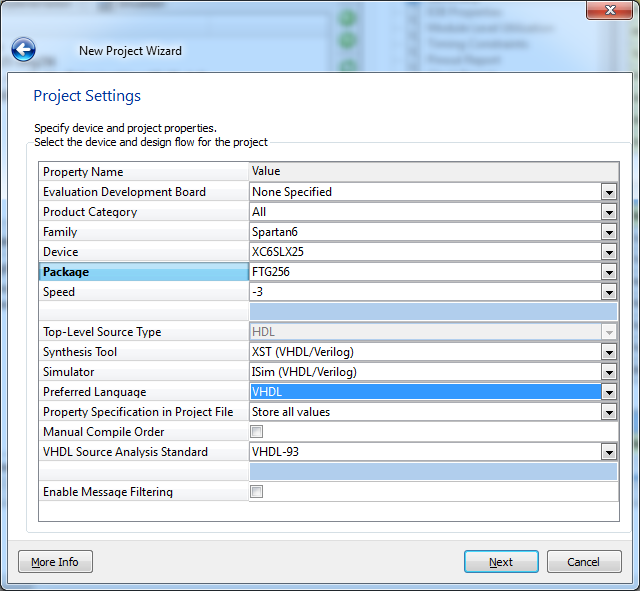 You get presented with settings to choose from when you initially create a new project, after giving it a name and description. IŌĆÖve set my project up for VHDL and the same chip on my miniSpartan6+ board. Once we accept these settings, we have the IDE ready for getting some VHDL modules added.
Making our VHDL module
In this part we want to concern ourselves with the register file. The registers, for this CPU, will come in the form of 8 16-bit values. IŌĆÖll go into more detail in the next part about Instruction Set Architecture choices, but for now we assume that we have a destination register value, and two sources for ALU operations.
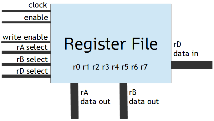 With the register file as a black box, we know it must have 3 inputs to it for indicating what registers we want for the destination and two sources. We also need the data output from those sources, and an input for the destination. Finally, we want control line for the write enable functionality of the register file. Sometimes we will not want the destination value to be actually written, so it needs an input to enable the writing of data. The inputs which select the registers will address one of 8, so we need a 3 bit signal for the selection lines. For the data, we know they are 16-bit wide. We will also need a clock input, and an enable bit. With this information fixed, we can create a new VHDL module within our project and detail the ports it exposes.
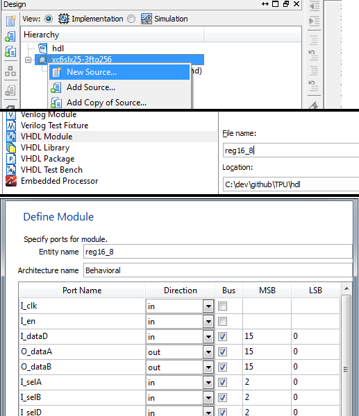 ISE creates the skeleton for the source automatically. The empty module is as follows.
entity reg16_8 is
Port ( I_clk : in┬Ā STD_LOGIC;
I_en : in┬Ā STD_LOGIC;
I_dataD : in┬Ā STD_LOGIC_VECTOR (15 downto 0);
O_dataA : out┬Ā STD_LOGIC_VECTOR (15 downto 0);
O_dataB : out┬Ā STD_LOGIC_VECTOR (15 downto 0);
I_selA : in┬Ā STD_LOGIC_VECTOR (2 downto 0);
I_selB : in┬Ā STD_LOGIC_VECTOR (2 downto 0);
I_selD : in┬Ā STD_LOGIC_VECTOR (2 downto 0);
I_we : in┬Ā STD_LOGIC);
end reg16_8;
architecture Behavioral of reg16_8 is
begin
end Behavioral;ItŌĆÖs worth noting at this point that IŌĆÖve used STD_LOGIC_VECTOR (SLV) types everywhere. Upon posting Part 1 of this series, I had a few folk tell me where possible to use the integer types. A quick Google for more information does show many folk using those instead of the raw SLV types for various reasons. I may go into those later, and revisit the code to re-implement with less SLV usage. For now, however, I intend to just crack on and continue regardless.
Register file logic
The register file is very simple. we need it to do the following
- On each clock cycle and if enabled, update the source A and B register outputs given the selection inputs for A and B
- On each clock cycle and if enabled, and if the write enable is active, set the internal value of the register D selected to that passed into the dataD input
For this, we will add a process block.
architecture Behavioral of reg16_8 is
begin
  process(I_clk)
  begin
    if rising_edge(I_clk) and I_en='1' then
      -- do our things!
    end if;
  end process;
end Behavioral;
We add I_clk into the process sensitivity list ŌĆō the parameters after the process keyword. This means this process gets re-evaluated when the state of I_clk changes, which is exactly what youŌĆÖd expect. The next thing we need to do is define our actual data store, the registers themselves. This is fairly easy and we just define a type, followed by a signal of that type.
architecture Behavioral of reg16_8 is
  type store_t is array (0 to 7) of std_logic_vector(15 downto 0);
  signal regs: store_t := (others => X"0000");
begin
  ..
regs is now an array of 8 SLVs containing 16 bits each ŌĆō representing our registers. The others statement initializes all bits to 0. Now we just add our logic as per to two main use cases above. We cast our standard_logic_vector inputs to unsigned integers as to index the regs signal array.
process(I_clk)
begin
if rising_edge(I_clk) and I_en='1' then
O_dataA <= regs(to_integer(unsigned(I_selA)));
O_dataB <= regs(to_integer(unsigned(I_selB)));
if (I_we = '1') then
regs(to_integer(unsigned(I_selD))) <= I_dataD;
end if;
end if;
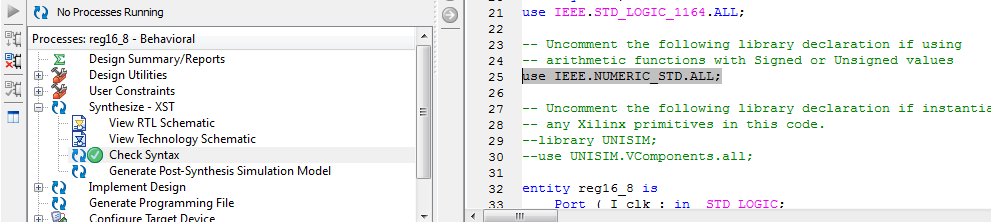
end process;At this point its worth checking our syntax using the command listed under Synthesize when the module is selected in the hierarchy within ISE. This will show a few errors, as we are using functionality that you need to include a library for. Thankfully, the generated module has inserted comments near the top of the file indicating all we need is to include the statement ŌĆśuse IEEE.NUMERIC_STD.ALL;ŌĆÖ to use these functions. Doing this will allow for our register file to pass syntax checking.

 Testing
To test our module, we will create a test bench for it within ISE. Right click the hierarchy, and add new source, of type VHDL Test Bench. I name my tests after what IŌĆÖm testing, with ŌĆś_tbŌĆÖ appended. But you can call it anything. Associate the test with the register file module, and a new VHDL file containing a test harness will be created based on itŌĆÖs definition ŌĆō ready for you to add in some detail.
 When simulating, you can assign values to the inputs and issue wait statements to account for cycle latencies. ISE automatically generates a clock process for you, so that input is taken care of. If we assign some values to the input, and attempt to write a value to a register D which is also one of the selected register A or B outputs, if we then wait a clock cycle we should see the output for register A change. This test looks as follows:
-- insert stimulus here
I_en <= '1';
I_selA <= "000";
I_selB <= "001";
I_selD <= "000";
I_dataD <= X"FAB5";
I_we <= '1';
wait for I_clk_period;
Now by running the ŌĆśSimulate Behavioural ModelŌĆÖ process when in Simulation view (which you should be now after editing the test bench source file) you get an ISim instance showing a waveform timeline of all the signals. Here we can validate out expected output, and we do get what was expected. After a single clock cycle, the output from register A (the O_dataA signal) becomes 0xFAB5.
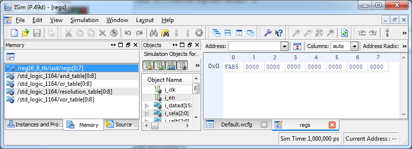
 You can view the contents of the regs array using the memory pane.
 We can extend the test a bit more, to cover some basic situations we know we will get to. Test further writes, make sure we do not write when the write enable is not asserted, writing multiple times to the same register, and finally reading the same register twice on the same clock cycle ŌĆō useful for nops (using or), doubling values with add and also clearing with xor. The output from the simulator is shown below, with some notes annotated at respective cycles. The full test bench source is at the end of this post.
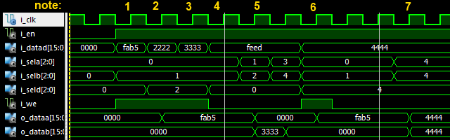
- read r0 and r1, write 0xfab5 to r0
- Ensure 0xfab5 appears on data out line, write 0x2222 to r2
- Write 0x3333 to r2, testing multiple writes to same location
- Set up as though writing 0xfeed to r0, but dont signal write enable
- Read r2, ensuring it is 0x3333 not 0x2222. Ensure r1 is 0x0. Ensure r3 and r4 are 0x0.
- Write 0x4444 to r4. ensure 0xfeed was not written to r0.
- after several cycles, read r4 on both A and B outputs, to test we can read the same register on both ports. Ensure the output is the 0x44 we wrote earlier, on both outputs.
This test shows us the register file should be suitable for our needs!
Moving on
A further test to add would be to also test the enable bit works (as in, when disabled nothing updates) ŌĆō youŌĆÖll have to trust me when I say it does! ItŌĆÖs worth noting there are VHDL asserts, but the truth is despite them compiling fine IŌĆÖve not found where any pass/fail/errors appear ŌĆō even when IŌĆÖve forced an assert condition to fail. Maybe someone could help me out in that regard (message @domipheus).
ThatŌĆÖs it for this part. Thanks for reading, comments as always to @domipheus, and the next part will be about the ISA and decoder!
The next part in the series is now available.
[Thanks to @EmptyJayy for pointing out some formatting issues and finding the correct ISE URL!]
Source for the test bench used in the annotated simulation is below.
LIBRARY ieee;
USE ieee.std_logic_1164.ALL;

-- Uncomment the following library declaration if using
-- arithmetic functions with Signed or Unsigned values
--USE ieee.numeric_std.ALL;

ENTITY reg16_8_tb IS
END reg16_8_tb;

ARCHITECTURE behavior OF reg16_8_tb IS

    -- Component Declaration for the Unit Under Test (UUT)

    COMPONENT reg16_8
    PORT(
         I_clk : IN  std_logic;
         I_en : IN  std_logic;
         I_dataD : IN  std_logic_vector(15 downto 0);
         O_dataA : OUT  std_logic_vector(15 downto 0);
         O_dataB : OUT  std_logic_vector(15 downto 0);
         I_selA : IN  std_logic_vector(2 downto 0);
         I_selB : IN  std_logic_vector(2 downto 0);
         I_selD : IN  std_logic_vector(2 downto 0);
         I_we : IN  std_logic
        );
    END COMPONENT;

   --Inputs
   signal I_clk : std_logic := '0';
   signal I_en : std_logic := '0';
   signal I_dataD : std_logic_vector(15 downto 0) := (others => '0');
   signal I_selA : std_logic_vector(2 downto 0) := (others => '0');
   signal I_selB : std_logic_vector(2 downto 0) := (others => '0');
   signal I_selD : std_logic_vector(2 downto 0) := (others => '0');
   signal I_we : std_logic := '0';

  --Outputs
   signal O_dataA : std_logic_vector(15 downto 0);
   signal O_dataB : std_logic_vector(15 downto 0);

   -- Clock period definitions
   constant I_clk_period : time := 10 ns;

BEGIN

  -- Instantiate the Unit Under Test (UUT)
   uut: reg16_8 PORT MAP (
          I_clk => I_clk,
          I_en => I_en,
          I_dataD => I_dataD,
          O_dataA => O_dataA,
          O_dataB => O_dataB,
          I_selA => I_selA,
          I_selB => I_selB,
          I_selD => I_selD,
          I_we => I_we
        );

   -- Clock process definitions
   I_clk_process :process
   begin
    I_clk <= '0';
    wait for I_clk_period/2;
    I_clk <= '1';
    wait for I_clk_period/2;
   end process;

   -- Stimulus process
   stim_proc: process
   begin
      -- hold reset state for 100 ns.
      wait for 100 ns;

      wait for I_clk_period*10;

      -- insert stimulus here

    I_en <= '1';

    -- test for writing.
    -- r0 = 0xfab5
    I_selA <= "000";
    I_selB <= "001";
    I_selD <= "000";
    I_dataD <= X"FAB5";
    I_we <= '1';
      wait for I_clk_period;

    -- r2 = 0x2222
    I_selA <= "000";
    I_selB <= "001";
    I_selD <= "010";
    I_dataD <= X"2222";
    I_we <= '1';
      wait for I_clk_period;

    -- r3 = 0x3333
    I_selA <= "000";
    I_selB <= "001";
    I_selD <= "010";
    I_dataD <= X"3333";
    I_we <= '1';
      wait for I_clk_period;

    --test just reading, with no write
    I_selA <= "000";
    I_selB <= "001";
    I_selD <= "000";
    I_dataD <= X"FEED";
    I_we <= '0';
      wait for I_clk_period;

    --at this point dataA should not be 'feed'

    I_selA <= "001";
    I_selB <= "010";
      wait for I_clk_period;

    I_selA <= "011";
    I_selB <= "100";
      wait for I_clk_period;

    I_selA <= "000";
    I_selB <= "001";
    I_selD <= "100";
    I_dataD <= X"4444";
    I_we <= '1';
      wait for I_clk_period;

    I_we <= '0';
      wait for I_clk_period;

    -- nop
      wait for I_clk_period;

    I_selA <= "100";
    I_selB <= "100";
      wait for I_clk_period;

      wait;
   end process;

END;